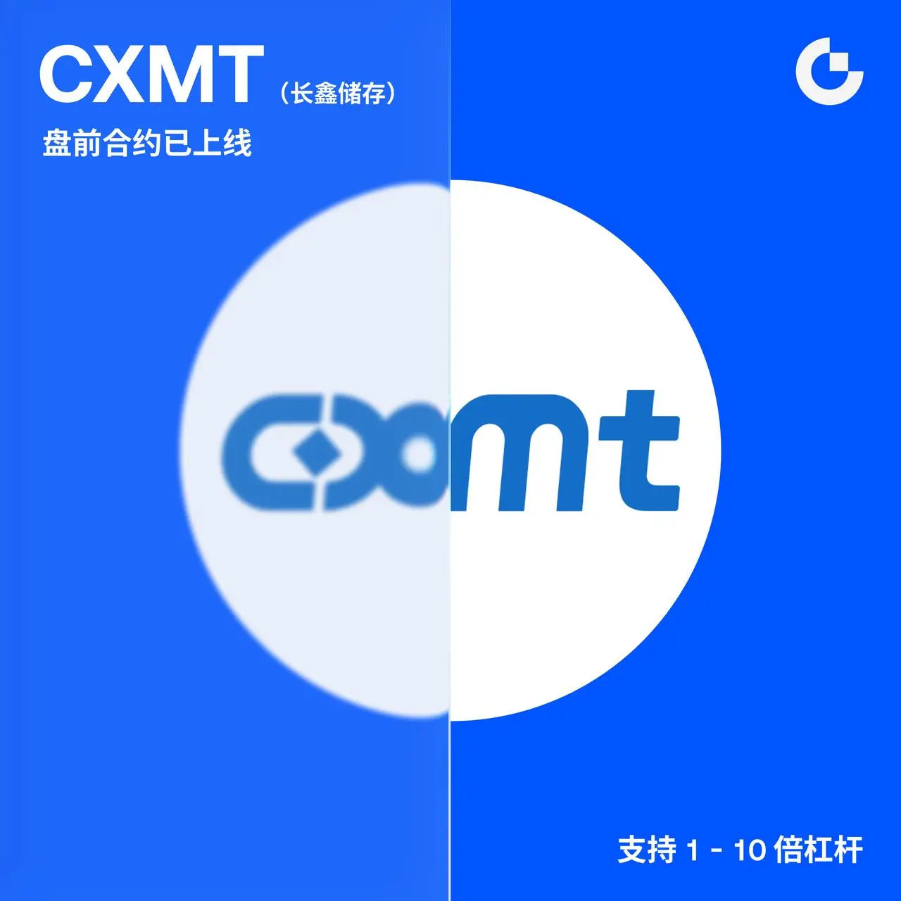





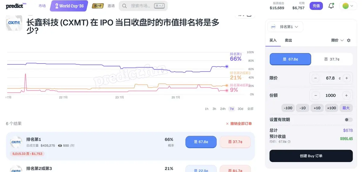
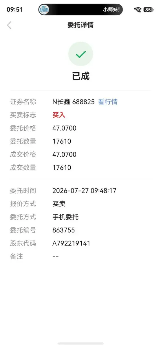
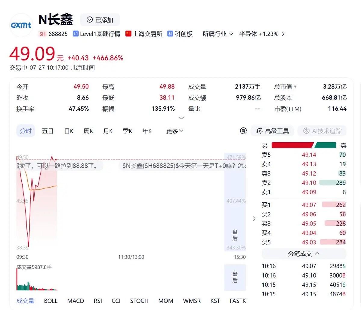




#长鑫今日上市Gate合约抢占交易先机 ChangXin Technology’s technological advantages:
1、"leapfrogging R&D" strategy—an aggressive jump instead of industry-standard iterative upgrades ChangXin did not choose the conventional generation-by-generation iteration roadmap. Instead, it adopted an aggressive leapfrogging R&D strategy: jumping directly from the first-generation process platform (18nm/1Xnm) to the fourth generation (about 13-14nm/1αnm), skipping the intermediate 1Ynm (16-17nm) transition process. This strategy is similar to Samsung’s approach years ago when it jumped from 64K directly to 4M/16M synchronous parallel R&D—overtaking Japan in one move: it does not chase step by step, but instead targets frontier nodes directly, compressing the time needed to catch up. To date, it has completed full product line coverage and iteration from DDR4 and LPDDR4X to DDR5 and LPDDR5/5X, and the fifth-generation process platform has also entered the R&D stage.
2、Bonded DRAM—bypassing the disruptive EUV route This is currently ChangXin’s most talked-about technical breakthrough. In July 2026, it was disclosed that ChangXin is secretly testing bonded DRAM pilot production lines in Hefei:
Core idea: split the storage cell array and peripheral control logic circuitry across different wafers, manufacture them separately, and then use "wafer-to-wafer hybrid bonding" (W2W Hybrid Bonding) to precisely align and fuse the two wafers
Key breakthrough: high-density DRAM can be produced using only DUV deep-ultraviolet lithography combined with multiple patterning, without relying on EUV extreme-ultraviolet lithography machines that have been banned due to U.S. export controls
Performance advantages: eliminate traditional microbumps, shorten interconnect length, reduce parasitic resistance and power consumption, improve transmission speed, and increase storage density without increasing wafer size
Progress: according to South Korean media reports, ChangXin may have already outpaced Samsung and SK hynix in bonded DRAM technology development speed
3、IDM vertical integration—end-to-end self-control across design, manufacturing, and packaging/testing. Unlike most Chinese semiconductor companies that only do chip design, ChangXin is the only 🇨🇳 DRAM company using an IDM model (design-manufacturing-packaging/testing integrated). Its structure is fully analogous to Samsung, SK hynix, and Micron.
This means:
From wafers to chips to modules, the entire workflow is independently controlled, with no disconnect between design and foundry work
It can quickly respond to customer customization needs (e.g., joint development with Alibaba Cloud and Tencent on server-dedicated memory solutions)
Yield issues on production lines can be closed-loop iterated internally, shortening the improvement cycle
4、Patent moat—inheritance plus independent accumulation. At the beginning of its establishment, ChangXin acquired a large number of foundational patents by purchasing a bankrupt German DRAM company, Qimonda (Qimonda), and inherited from it, avoiding the first wave of blockade by the patent “three giants” surrounding it. Since then, it has continued to accumulate independently. As of the end of 2025, the total number of patents across all categories is 6,972, including 3,165 domestic invention patents and 3,043 overseas patents, forming its own patent defense system and laying the foundation for future product overseas expansion.
5、Coordinated domestic equipment—supply-chain localization driven by "mass-production verification." ChangXin’s mass production lines provide a key production-line validation platform for domestically made semiconductor equipment:
At present, the overall share of domestic equipment on mass production lines is about 40-50%, and the localization rate for the next-generation platform is expected to exceed 40%
Deep joint R&D with North Huachuang (etching / thin-film deposition), AMEC (ultra-high aspect ratio etching), NAURA? (PECVD/ALD), and Huawei Haiqing? (CMP) etc. (as named in the source: 拓荆科技 and 华海清科)
Increasing the localization rate directly reduces costs: in 2023-2025, the unit price of silicon wafer procurement fell by about 30%, target materials fell by 22%, spare parts fell by 47%, and chemicals fell by 26% This kind of bundled model of "ChangXin + local supply chain" not only lowers costs and supply risk, but also forms a closed-loop “equipment localization replacement flywheel”—ChangXin expands capacity → domestic equipment verification → equipment vendors’ technical iteration → ChangXin’s next-generation production lines achieve an even higher localization rate.
6、HBM forward-looking deployment—charging into a high value-added track Although ChangXin has an approximately 3-year generational gap versus Samsung/SK hynix in the HBM field, it has been actively planning:
Developing next-generation frontier products such as CXL memory in parallel
Bonded DRAM technology itself is the foundation for 3D-stacked DRAM, and the wafer-bonding process for HBM is highly homologous; thus, technical accumulation can be reused in both directions
7、High-intensity R&D investment—use "R&D density" to make up for being late to start. From 2023-2025, ChangXin’s 3-year cumulative R&D investment was 20.6 billion yuan (earlier data shows 18.8 billion yuan over 3.5 years), with 6,259 R&D personnel (32.43% of employees). R&D spending as a proportion of revenue exceeds 20%, far above the 10%-15% level of overseas giants. This high-intensity R&D replicates the characteristics of Japan’s VLSI project and the period when Samsung chased up—compressing the technology gap by deploying an excessive R&D density.
8、Certainty of local demand—"home-field advantage" creates a commercial moat. Technical advantages ultimately need commercial scenarios to verify and iterate. ChangXin is backed by 🇨🇳 the world’s largest consumer electronics and cloud computing markets:
Domestic smartphone brands such as Xiaomi, OPPO, vivo, Honor, etc. have LPDDR adoption ratios exceeding 30%
Cloud providers such as Alibaba Cloud, ByteDance, and Tencent: the revenue share of their DDR-series jumped from 13% to 28%. It is based on long-term supply agreements signed with customers, and production capacity expansion is built on "substantive replacement share" rather than global spot price fluctuations
This kind of "certainty of localized demand" gives ChangXin’s technology iterations real shipment-volume validation, not just paper R&D.
In summary, ChangXin Technology’s technological strengths are not a single-point breakthrough, but a systemic catch-up strategy: leapfrogging R&D to compress timelines, using bonded DRAM to bypass EUV lockouts, the IDM model to guarantee full-chain independence, patent-moat defense to thwart blockades, coordinated domestic equipment to form a supply-chain flywheel, and using R&D intensity to exchange for speed. Local demand provides validation scenarios. Its core logic is, under constraints from U.S. export controls, to gradually narrow the gap with the three giants by "overtaking by taking a detour" rather than "chasing straight on." $CXMT
1、"leapfrogging R&D" strategy—an aggressive jump instead of industry-standard iterative upgrades ChangXin did not choose the conventional generation-by-generation iteration roadmap. Instead, it adopted an aggressive leapfrogging R&D strategy: jumping directly from the first-generation process platform (18nm/1Xnm) to the fourth generation (about 13-14nm/1αnm), skipping the intermediate 1Ynm (16-17nm) transition process. This strategy is similar to Samsung’s approach years ago when it jumped from 64K directly to 4M/16M synchronous parallel R&D—overtaking Japan in one move: it does not chase step by step, but instead targets frontier nodes directly, compressing the time needed to catch up. To date, it has completed full product line coverage and iteration from DDR4 and LPDDR4X to DDR5 and LPDDR5/5X, and the fifth-generation process platform has also entered the R&D stage.
2、Bonded DRAM—bypassing the disruptive EUV route This is currently ChangXin’s most talked-about technical breakthrough. In July 2026, it was disclosed that ChangXin is secretly testing bonded DRAM pilot production lines in Hefei:
Core idea: split the storage cell array and peripheral control logic circuitry across different wafers, manufacture them separately, and then use "wafer-to-wafer hybrid bonding" (W2W Hybrid Bonding) to precisely align and fuse the two wafers
Key breakthrough: high-density DRAM can be produced using only DUV deep-ultraviolet lithography combined with multiple patterning, without relying on EUV extreme-ultraviolet lithography machines that have been banned due to U.S. export controls
Performance advantages: eliminate traditional microbumps, shorten interconnect length, reduce parasitic resistance and power consumption, improve transmission speed, and increase storage density without increasing wafer size
Progress: according to South Korean media reports, ChangXin may have already outpaced Samsung and SK hynix in bonded DRAM technology development speed
3、IDM vertical integration—end-to-end self-control across design, manufacturing, and packaging/testing. Unlike most Chinese semiconductor companies that only do chip design, ChangXin is the only 🇨🇳 DRAM company using an IDM model (design-manufacturing-packaging/testing integrated). Its structure is fully analogous to Samsung, SK hynix, and Micron.
This means:
From wafers to chips to modules, the entire workflow is independently controlled, with no disconnect between design and foundry work
It can quickly respond to customer customization needs (e.g., joint development with Alibaba Cloud and Tencent on server-dedicated memory solutions)
Yield issues on production lines can be closed-loop iterated internally, shortening the improvement cycle
4、Patent moat—inheritance plus independent accumulation. At the beginning of its establishment, ChangXin acquired a large number of foundational patents by purchasing a bankrupt German DRAM company, Qimonda (Qimonda), and inherited from it, avoiding the first wave of blockade by the patent “three giants” surrounding it. Since then, it has continued to accumulate independently. As of the end of 2025, the total number of patents across all categories is 6,972, including 3,165 domestic invention patents and 3,043 overseas patents, forming its own patent defense system and laying the foundation for future product overseas expansion.
5、Coordinated domestic equipment—supply-chain localization driven by "mass-production verification." ChangXin’s mass production lines provide a key production-line validation platform for domestically made semiconductor equipment:
At present, the overall share of domestic equipment on mass production lines is about 40-50%, and the localization rate for the next-generation platform is expected to exceed 40%
Deep joint R&D with North Huachuang (etching / thin-film deposition), AMEC (ultra-high aspect ratio etching), NAURA? (PECVD/ALD), and Huawei Haiqing? (CMP) etc. (as named in the source: 拓荆科技 and 华海清科)
Increasing the localization rate directly reduces costs: in 2023-2025, the unit price of silicon wafer procurement fell by about 30%, target materials fell by 22%, spare parts fell by 47%, and chemicals fell by 26% This kind of bundled model of "ChangXin + local supply chain" not only lowers costs and supply risk, but also forms a closed-loop “equipment localization replacement flywheel”—ChangXin expands capacity → domestic equipment verification → equipment vendors’ technical iteration → ChangXin’s next-generation production lines achieve an even higher localization rate.
6、HBM forward-looking deployment—charging into a high value-added track Although ChangXin has an approximately 3-year generational gap versus Samsung/SK hynix in the HBM field, it has been actively planning:
Developing next-generation frontier products such as CXL memory in parallel
Bonded DRAM technology itself is the foundation for 3D-stacked DRAM, and the wafer-bonding process for HBM is highly homologous; thus, technical accumulation can be reused in both directions
7、High-intensity R&D investment—use "R&D density" to make up for being late to start. From 2023-2025, ChangXin’s 3-year cumulative R&D investment was 20.6 billion yuan (earlier data shows 18.8 billion yuan over 3.5 years), with 6,259 R&D personnel (32.43% of employees). R&D spending as a proportion of revenue exceeds 20%, far above the 10%-15% level of overseas giants. This high-intensity R&D replicates the characteristics of Japan’s VLSI project and the period when Samsung chased up—compressing the technology gap by deploying an excessive R&D density.
8、Certainty of local demand—"home-field advantage" creates a commercial moat. Technical advantages ultimately need commercial scenarios to verify and iterate. ChangXin is backed by 🇨🇳 the world’s largest consumer electronics and cloud computing markets:
Domestic smartphone brands such as Xiaomi, OPPO, vivo, Honor, etc. have LPDDR adoption ratios exceeding 30%
Cloud providers such as Alibaba Cloud, ByteDance, and Tencent: the revenue share of their DDR-series jumped from 13% to 28%. It is based on long-term supply agreements signed with customers, and production capacity expansion is built on "substantive replacement share" rather than global spot price fluctuations
This kind of "certainty of localized demand" gives ChangXin’s technology iterations real shipment-volume validation, not just paper R&D.
In summary, ChangXin Technology’s technological strengths are not a single-point breakthrough, but a systemic catch-up strategy: leapfrogging R&D to compress timelines, using bonded DRAM to bypass EUV lockouts, the IDM model to guarantee full-chain independence, patent-moat defense to thwart blockades, coordinated domestic equipment to form a supply-chain flywheel, and using R&D intensity to exchange for speed. Local demand provides validation scenarios. Its core logic is, under constraints from U.S. export controls, to gradually narrow the gap with the three giants by "overtaking by taking a detour" rather than "chasing straight on." $CXMT