In 2026, advanced packaging continues to be a major focus of the semiconductor industry. TSMC introduced a roadmap for larger-scale CoWoS packaging at its annual technology symposium, with plans to integrate more compute chiplets and HBM by expanding the package size. Meanwhile, TrendForce noted in September that as AI accelerator sizes increase, CoWoS-L is expected to remain an important packaging solution for high-end AI chips over the next several years.
For NVIDIA, AMD, and other AI chip suppliers, even if they can obtain sufficient advanced-node wafers, a shortage of HBM or advanced packaging capacity could still prevent them from completing product deliveries as planned. Therefore, understanding CoWoS not only helps explain how AI chips are manufactured but also helps investors analyze capacity constraints, technological competition, and business opportunities across the semiconductor supply chain.
Key Takeaways
-
CoWoS is TSMC's advanced packaging technology. It uses high-density interconnect structures to integrate GPUs, AI accelerator compute chiplets, and high-bandwidth memory (HBM) in the same package.
-
AI chip output depends on more than GPU wafers. Advanced-node wafers, HBM, CoWoS packaging capacity, and package substrates can all affect the final number of products delivered.
-
CoWoS-S, CoWoS-L, and CoWoS-R use different interconnect structures. As AI chips grow larger, CoWoS-L is becoming an important packaging solution for large AI accelerators.
-
NVIDIA, AMD, and cloud service providers are all competing for advanced packaging resources. The development of AI GPUs and custom ASICs means that demand for CoWoS is no longer limited to a single chipmaker.
-
CoWoS capacity expansion could affect the semiconductor supply chain. However, increased packaging demand does not mean that all related companies will achieve the same level of profit growth. Technology capabilities, orders, and valuations still require careful consideration.
What Is CoWoS, and How Does It Differ From Traditional Chip Packaging?
CoWoS stands for Chip-on-Wafer-on-Substrate. It is an advanced 2.5D packaging technology whose core function is to connect multiple chips or chiplets through high-density interconnect structures so that they can work together in the same package. Unlike designs that concentrate all functions in a single large chip, CoWoS can combine compute chips, memory, and other components into a more complex system.
Traditional chip packaging primarily protects the chip, connects it to external circuits, and provides power delivery and heat dissipation paths. In some traditional packaging solutions, processors and memory communicate through circuit boards outside the package. As AI computing demands higher data transfer speeds, this type of connection may face limitations in bandwidth, latency, and power consumption. CoWoS, by contrast, uses an interposer or other high-density interconnect structures to shorten the distance between different chips and improve data exchange efficiency.
For example, a large accelerator designed for AI training may need to connect to multiple HBM stacks at the same time. CoWoS can install the compute chip and HBM in the same package structure and use dense metal interconnects to enable high-speed communication. This design does not mean that the GPU and HBM are manufactured as a single chip. Instead, advanced packaging creates a closely integrated computing system. TSMC includes CoWoS in its 3DFabric technology platform and continues to expand its packaging structures to meet the needs of high-performance computing and AI applications.
How Does CoWoS Integrate GPUs, HBM, and Interposers?
The core structure of CoWoS typically includes logic compute chips, HBM, high-density interconnect structures, and a package substrate. The logic chip performs AI computations, HBM provides high-speed data access, and the interposer or local interconnect structure connects the signals between different chips. The package substrate then connects the entire module to the server motherboard and supports power delivery and signal transmission.
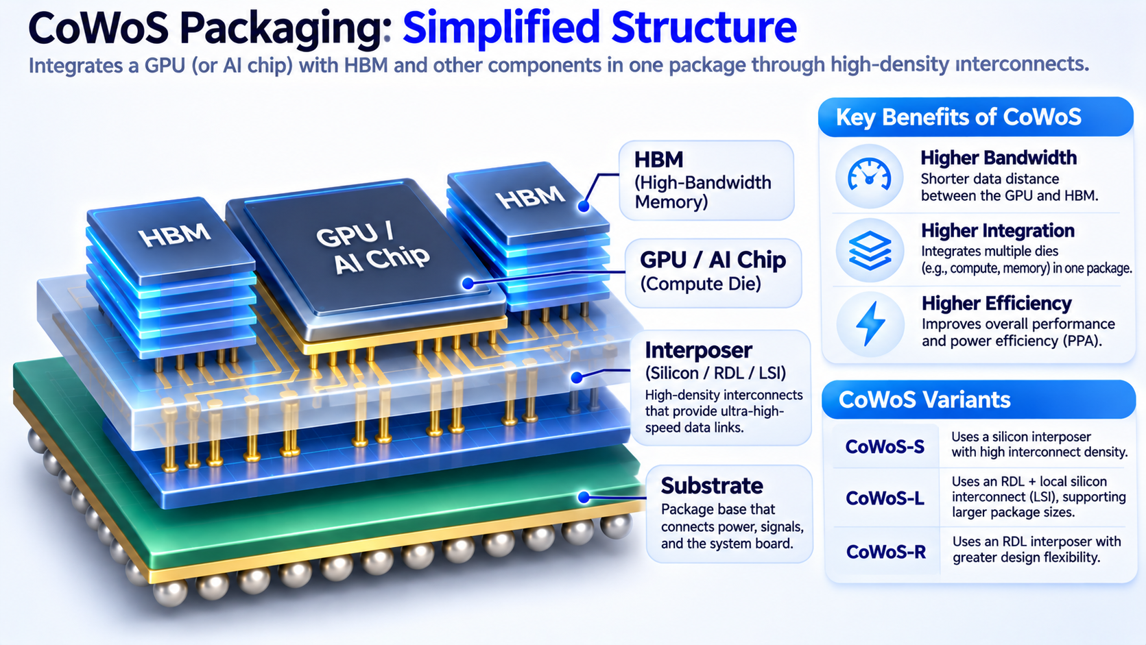
HBM is a key component of this structure. Compared with conventional server memory, HBM stacks multiple layers of DRAM chips and uses a wide interface to provide very high memory bandwidth within a relatively small package footprint. For AI inference tasks that frequently read model parameters and training tasks that require extensive data exchange, HBM can help relieve some memory access bottlenecks.
However, HBM can deliver its full performance only when the compute chip can access it efficiently. CoWoS uses dense interconnects to connect the compute chip with multiple HBM stacks, allowing data to travel over shorter distances. This can not only increase bandwidth but also improve energy efficiency in certain data transfer processes.
Therefore, the performance of an advanced AI accelerator depends on multiple factors, including the compute architecture, HBM configuration, packaging interconnects, and system software. Even if a GPU has very high theoretical computing power, its real-world application performance may still be limited if memory bandwidth is insufficient or data transfer efficiency is low.
What Are the Differences Between CoWoS-S, CoWoS-L, and CoWoS-R?
TSMC currently offers three major technology solutions: CoWoS-S, CoWoS-L, and CoWoS-R. They share the goal of achieving high-density chip integration but differ in their interposer structures, scalability, and applicable use cases.
| Technology Type |
Core Structure |
Main Features |
| CoWoS-S |
Silicon interposer |
High-density interconnects, suitable for high-performance computing |
| CoWoS-L |
RDL interposer structure + local silicon interconnect (LSI) |
Supports larger package sizes and multi-chip integration |
| CoWoS-R |
RDL interposer |
Uses polymer and copper interconnect structures, providing design flexibility |
CoWoS-S is a relatively mature solution. It uses a large silicon interposer to connect compute chips and HBM, providing high interconnect density. As AI accelerators continue to add compute chiplets and HBM stacks, the required package area also continues to grow. The manufacturing difficulty, cost, and size limitations of large silicon interposers are gradually becoming issues that need to be addressed.
CoWoS-L combines redistribution layers with local silicon interconnect structures. It provides high-density interconnects where high-speed connections are needed while supporting a larger package area. TSMC's CoWoS-L entered mass production in 2024 and continues to evolve toward larger sizes. In a 2026 study, TrendForce stated that CoWoS-L is expected to maintain its important position in advanced packaging for high-end AI chips through 2028, supported by its technological maturity and yield advantages.
CoWoS-R uses an RDL interposer based on polymer and copper interconnects, providing more flexible design options in certain applications. It is important to note that none of the three solutions has an absolute performance ranking that applies to every product. Chip designers need to select the appropriate solution based on interconnect density, package size, manufacturing costs, yield, and product requirements.
Why Does AI Chip Demand Depend on More Than GPU Capacity?
AI chip manufacturing involves multiple interconnected stages. First, a chip design company completes the architecture for a GPU or AI accelerator. A foundry then uses an advanced process to manufacture the compute chip. At the same time, memory manufacturers need to provide HBM that meets the required specifications, while packaging manufacturers integrate the compute chip with the memory. The product then goes through testing, substrate assembly, and other processes before it becomes deliverable.
This means that GPU wafer output represents only part of AI chip supply capacity. Suppose a company plans to produce 100,000 AI accelerators and has obtained enough compute chips, but the available HBM can support only 80,000 products and advanced packaging capacity can support only 60,000. In that case, the final number of completed products may be limited by the packaging stage. This example is provided only to explain supply chain constraints and does not represent the actual production data of any company.
In March 2026, a study published by Epoch AI estimated that in 2025, NVIDIA, Google, AMD, and Amazon—the four major AI chip designers and purchasers—collectively consumed more than 90% of global CoWoS capacity and HBM supply, while accounting for a relatively smaller share of advanced logic chiplet output. This indicates that during certain periods, advanced packaging and HBM may be more constrained than advanced logic wafer supply in the conventional sense. It is important to note that the study used an estimation model, and its results do not represent the actual capacity utilization rates of all manufacturers.
Therefore, analyzing AI chip supply requires more than monitoring TSMC's 3nm or 2nm wafer capacity. It is also necessary to consider HBM deliveries, packaging yield, substrate supply, and testing capacity. Capacity expansion rates differ across stages, and delays at any critical stage could affect the launch and delivery timelines of final products.
Why Are NVIDIA, AMD, and Cloud Service Providers Competing for CoWoS Capacity?
As demand for AI computing grows, NVIDIA and AMD both need more advanced packaging resources to support their next-generation GPU products. At the same time, major technology companies such as Google, Amazon, Microsoft, and Meta are developing their own AI accelerators. Although these products use different computing architectures, some also require HBM and advanced packaging technologies, creating shared demand across the relevant supply chain.
For NVIDIA, CoWoS capacity is closely linked to the shipment capacity of high-end AI GPUs. GPUs need to be packaged together with HBM before they can be further integrated into server- and rack-scale systems. Even if market demand for AI accelerators is strong, insufficient packaging capacity may require companies to adjust their delivery schedules. AMD faces similar challenges, as the development of its Instinct products also requires coordination across wafer, HBM, packaging, and substrate resources.
In September 2026, TrendForce stated that NVIDIA was continuing to advance large-scale AI rack systems, while AMD was actively promoting its MI400/MI450 series products. At the same time, Google's TPU, Amazon's Trainium, and other cloud service providers' in-house ASICs were expanding their deployments. Different products use different packaging solutions, but the overall trend is that more AI chip suppliers need high-density packaging and high-speed memory resources.
This competition does not mean that every AI chip must use CoWoS. Alternative technologies such as Intel's EMIB are also developing, and some chips can use different packaging solutions. The key point is that high-end AI computing continues to demand greater chip interconnect density, package area, and memory bandwidth, making advanced packaging an increasingly important supply chain resource.
Why Is CoWoS Capacity Difficult to Expand Quickly?
Expanding advanced packaging capacity involves more than adding equipment. CoWoS includes multiple complex processes, such as high-precision manufacturing, chip placement, interconnect structure processing, material handling, and reliability testing. As package areas grow and the number of chiplets increases, manufacturers must control more process variables, placing higher demands on equipment precision, yield, and supply chain coordination.
Packaging yield is an important factor. Suppose a large package module contains multiple high-value compute chiplets and HBM stacks. A defect at a critical manufacturing step could affect the usability of the entire module. The more complex the package structure, the more manufacturers need to optimize their processes, inspection, and rework procedures. Therefore, it typically takes time for a new packaging production line to progress from construction to stable mass production. Planned capacity cannot simply be equated with actual shipment capacity.
In addition, CoWoS capacity expansion is affected by upstream equipment, package substrates, materials, and human resources. In April 2026, TrendForce stated that demand for AI chips had expanded supply pressures from advanced wafer manufacturing to packaging equipment, substrates, and related materials. Even if TSMC continues to increase its packaging capacity, slower expansion across supporting suppliers could create new bottlenecks.
For chipmakers, this also explains why long-term capacity planning is becoming increasingly important. Companies need to coordinate with foundries, memory manufacturers, and packaging suppliers in advance to ensure that the required resources are available across different manufacturing stages at roughly the same time. Otherwise, increased capacity at one stage may not immediately translate into higher shipments of final AI chips.
How Is TSMC Expanding CoWoS Capacity? What Are the New Developments in 2026?
TSMC is expanding package sizes, optimizing interconnect structures, and increasing production capacity to meet the computing performance and memory capacity requirements of next-generation AI accelerators. As individual AI accelerators integrate more chiplets and HBM, package areas continue to grow, making the size limitations of traditional interposers a major technical challenge.
In May 2026, TSMC introduced larger CoWoS technologies at a technology symposium and stated that it had begun producing a CoWoS solution measuring 5.5 times the reticle size. This multiple describes the package scale relative to the standard reticle exposure area. It does not mean that computing performance increases by the same multiple. The primary significance of expanding the package size is that it allows more compute chips and memory components to be integrated into the same package.
TSMC CoWoS Technology Expansion Roadmap
| 2024 |
The CoWoS-L 3.5x reticle-size solution entered mass production |
| 2026 |
Advancing production of 5.5x reticle-size CoWoS |
| 2028 (planned) |
Introducing a solution measuring approximately 14x the reticle size, capable of integrating approximately 10 large compute chiplets and 20 HBM stacks |
| 2029 (planned) |
Further expanding beyond 14x the reticle size |
Source: TSMC CoWoS technology documentation and the 2026 technology symposium. Future timelines are plans and do not indicate completed mass production.
These developments reflect changes in how AI chips are scaling. In the past, adopting more advanced transistor manufacturing processes was an important way to improve computing performance. Today, manufacturers can also improve system capabilities by expanding package sizes and increasing the number of chiplets and HBM stacks. However, larger packages may also create challenges involving manufacturing costs, power delivery, heat dissipation, and yield. The actual commercial value of these technology roadmaps still needs to be assessed based on mass-production performance.
What Is the Relationship Between CoWoS, HBM, Chiplets, and Advanced Processes?
CoWoS, HBM, chiplets, and advanced processes often appear together in discussions about the AI chip industry, but they are not the same technology concepts. Advanced processes primarily affect transistor density, performance, and power consumption in logic chips. Chiplets are a design method that divides a complex chip system into multiple chiplets. HBM provides high-bandwidth memory. CoWoS integrates these components in the same package through high-density interconnects.
For example, an AI accelerator can use an advanced process to manufacture compute chiplets and then connect multiple chiplets with HBM through CoWoS. This design can, to some extent, overcome the limitations that a single large chip faces in terms of manufacturing size and system integration. However, chiplets do not necessarily require CoWoS, and HBM is not essential for every AI chip. The specific architecture depends on performance targets, manufacturing costs, and product use cases.
From a supply chain perspective, these technologies are highly complementary. Advanced processes determine the foundational capabilities of compute chips, HBM provides data bandwidth, and advanced packaging determines how efficiently multiple components can work together. Therefore, the development of the AI chip industry cannot be attributed simply to continued process-node shrinkage. It requires coordinated optimization across chip design, manufacturing, memory, and packaging.
Which Semiconductor Companies Could Be Affected by Growing CoWoS Demand?
Growing demand for CoWoS first affects foundries and advanced packaging companies. TSMC not only manufactures large volumes of advanced logic chips but also provides CoWoS packaging services, allowing it to participate in multiple stages, from front-end manufacturing to back-end integration. However, expanding advanced packaging capacity generally requires substantial capital investment. Its contribution to profits still depends on capacity utilization, manufacturing yield, customer pricing, and depreciation costs.
HBM and semiconductor materials suppliers are another group that could be affected. Companies such as SK hynix, Samsung, and Micron participate in the high-bandwidth memory market, while suppliers of advanced package substrates, equipment, and related materials may also benefit from growing demand for AI computing. However, companies differ in their product mixes, technological capabilities, and customer structures. The entire supply chain should not be treated as a single growth category.
For NVIDIA and AMD, expanded CoWoS capacity could improve the supply conditions for high-end AI accelerators. If packaging resources become more readily available, chipmakers may find it easier to fulfill customer orders. However, improved supply could also change pricing and the competitive landscape. In particular, as more AI GPUs and custom ASICs enter the market, advanced packaging resources may become less constrained, and competition among manufacturers may focus more on actual performance, system costs, and software ecosystems.
Therefore, investors should not infer that a company's revenue or stock price will necessarily rise simply because it belongs to the CoWoS supply chain. More important factors include the company's specific role in the supply chain, technological barriers, capacity expansion plans, customer concentration, and future changes in profit margins.
How Can Investors Determine Whether CoWoS Capacity Expansion Is Creating Real Investment Opportunities?
Investors following TSMC and AI semiconductor stocks need to distinguish between market demand, capacity plans, and actual deliveries. Growing demand for CoWoS indicates that customers want more advanced packaging resources, but planned new capacity must go through equipment installation, process validation, and yield improvement before it can gradually become saleable output.
Investors can monitor capacity utilization and product mix. If advanced packaging capacity remains highly utilized over an extended period, related companies may have favorable business growth opportunities. However, if the industry expands capacity aggressively while actual AI chip demand falls short of expectations, capacity utilization could decline. Manufacturing costs and product pricing may also differ across CoWoS technology solutions. Profitability cannot be assessed based solely on package area or capacity volume.
Company valuations and market expectations also need to be considered. Semiconductor stock prices often reflect growth expectations for the next several quarters or even longer periods in advance. Even if CoWoS demand continues to grow, if a company's stock price has already fully priced in optimistic expectations, actual financial performance may still fail to drive further valuation increases.
For individual investors, CoWoS is better viewed as an analytical tool for understanding the AI semiconductor supply chain rather than as an independent buy or sell signal. A more comprehensive assessment of industry changes requires considering advanced packaging together with HBM, wafer foundries, GPU shipments, customer capital expenditures, and corporate profit margins.
Summary
CoWoS is an important advanced packaging technology that TSMC uses for high-performance computing and AI accelerators. Through high-density interconnect structures, it integrates GPUs, compute chiplets, and HBM in the same package. It addresses more than chip assembly. It also affects data transfer efficiency between computing and memory, system performance, and manufacturing scalability.
As NVIDIA, AMD, and major cloud service providers continue developing AI accelerators, advanced packaging has become an important factor affecting chip supply. Even if advanced-node wafer supply is sufficient, bottlenecks in HBM, CoWoS, or package substrates could still limit final product deliveries.
In the future, as CoWoS-L, large-package technologies, and other advanced packaging solutions continue to develop, competition among AI chips will depend increasingly on coordination across manufacturing, memory, and system integration capabilities. For semiconductor investors, understanding CoWoS provides a way to examine the real supply and demand dynamics of the AI industry beyond GPUs. However, assessments still need to incorporate corporate earnings, capacity utilization, and stock valuations.
FAQ
What Is CoWoS?
CoWoS is an advanced packaging technology developed by TSMC. It integrates compute chips with components such as HBM in the same package through high-density interconnect structures. It is primarily used in AI and high-performance computing.
Is CoWoS 2.5D or 3D Packaging?
CoWoS is generally classified as an advanced 2.5D packaging technology. It can connect multiple chips in the same package and can also integrate HBM, which uses internal 3D stacking structures. However, CoWoS should not be equated directly with all 3D chip-stacking technologies.
What Is the Difference Between CoWoS and HBM?
HBM is a high-bandwidth memory technology, while CoWoS is an advanced packaging technology. HBM provides high-speed data access, while CoWoS helps establish high-density interconnects between compute chips and HBM.
Why Does CoWoS Affect the Supply of NVIDIA and AMD GPUs?
High-end AI GPUs typically need to be packaged with HBM before they can be delivered. If CoWoS capacity is insufficient, compute chips that have already been manufactured may still be unable to become final products on schedule.
Why Is CoWoS-L Becoming Increasingly Important?
CoWoS-L can support larger-scale chip integration through RDL and local silicon interconnect structures, meeting next-generation AI accelerators' demand for more compute chiplets and HBM.
Does Increased CoWoS Capacity Mean That TSMC's Stock Price Will Definitely Rise?
Not necessarily. Capacity expansion may create business opportunities, but stock performance also depends on capital expenditures, manufacturing costs, capacity utilization, profitability, and market valuation.